Personal · Audio Arduino Club
Class-D
Audio Amp.
Explore audio amplification with a switching output stage.
A TPA3122-based amplifier I built in Audio Arduino Club under Dr. Gary Tuttle, with output filtering and configurable hardware controls.
Situation
Explore another amplifier architecture
This club project introduced the TPA3122 Class-D design alongside the analog amplifier builds. Its switching output stage brings filtering and power-supply components into sharper focus.
Task
Build the TPA3122 amplifier board
I assembled the club’s amplifier design under Dr. Gary Tuttle’s guidance. The task involved identifying a larger set of capacitors and understanding how the power, control, and output sections fit together.
Action
Assemble the filters and controls
The build starts with resistors and small capacitors, followed by connectors, the IC socket, output inductors, and control headers. Bootstrap and bypass capacitors support the chip, while the output filter and coupling components connect it to the speakers. Jumpers select gain and control mute and shutdown.
A switching amplifier with external filtering
The TPA3122 handles the Class-D amplification, while the surrounding circuit provides power conditioning, bootstrap support, and speaker-output filtering. Unlike the GTDT’s discrete output transistors, much of the active output circuitry is inside the amplifier IC. External inductors and capacitors remain important parts of the output path.
| Component / setting | Value and purpose |
|---|---|
| Control resistors | Four 10 kΩ pull-ups for gain, mute, and shutdown; a 1 kΩ LED resistor and two 4.7 kΩ output-filter resistors. |
| Bootstrap & local bypass | C7/C12: 0.22 µF bootstrap capacitors. C10: 10 µF; C5/C8/C14: 0.1 µF local bypass capacitors. |
| Signal & chip support | Four 1 µF capacitors: C3/C4 couple the inputs, while the other two serve VCLAMP and BYPASS. |
| Output filtering | L1/L2 inductors paired with 0.68 µF capacitors C15/C16; C17/C18 are 470 µF output-coupling capacitors. |
| Power conditioning | Bridge rectifier, 15 V regulator with 0.22 µF C2, 3300 µF input smoothing capacitor C1, and 470 µF supply bypass capacitors C6/C13. |
Build process
- Sort and install the smaller parts
Identify the resistor values and capacitor markings before soldering. The guide uses 224 for 0.22 µF, 104 for 0.1 µF, 105 for 1 µF, and 684 for 0.68 µF, making part identification a central assembly task.
- Build the output and control sections
Install the connectors, 20-pin socket, output inductors, and four jumper headers. Add the regulator, LED, and larger electrolytic capacitors, checking polarity and component alignment.
- Check power before inserting the IC
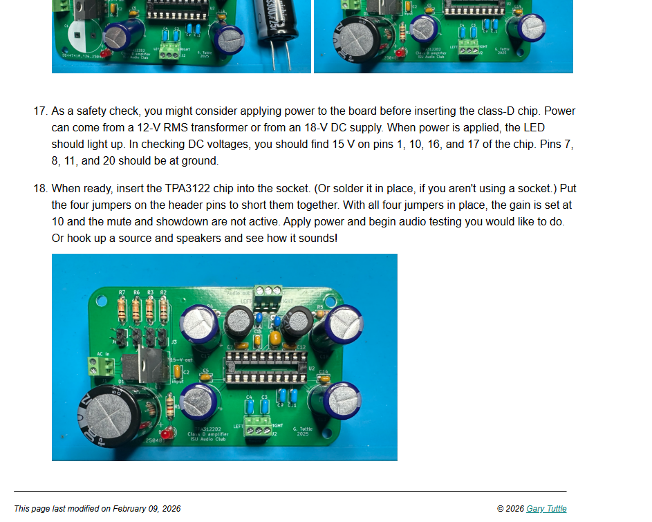
The guide recommends verifying 15 V at socket pins 1, 10, 16, and 17 and ground at pins 7, 8, 11, and 20. With the chip installed, all four jumpers select a gain of 10 and leave mute and shutdown inactive. These are the guide’s setup checks, not reported measurements from my build.
Result
Add switching-amplifier experience
I completed the Class-D amplifier project as part of my club work. The build expanded my experience with component placement, output filtering, and hardware configuration across different audio amplifier designs.
Design & build process
From components to a complete board.
Reference photographs from Dr. Gary Tuttle’s TPA3122 Class-D amplifier build guide, supplied as screenshots. These show the club’s reference builds.
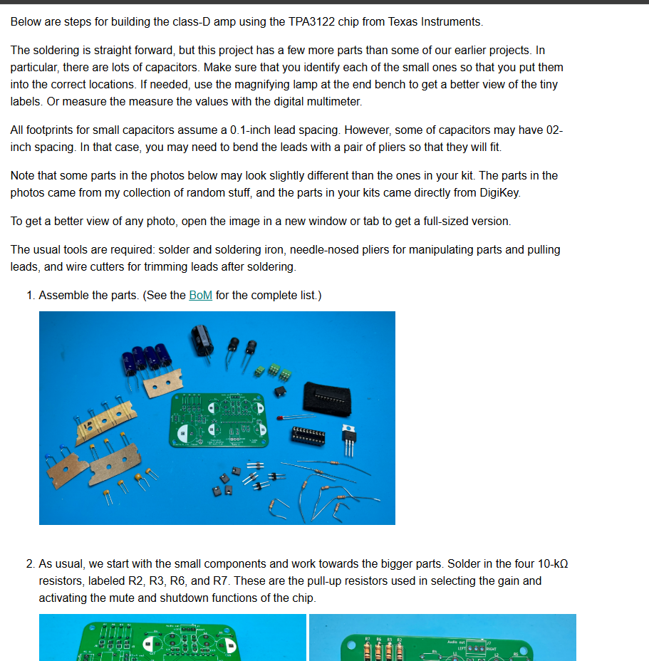
01 / Parts & layout
The kit includes the TPA3122, inductors, a socket, and a larger selection of capacitors.
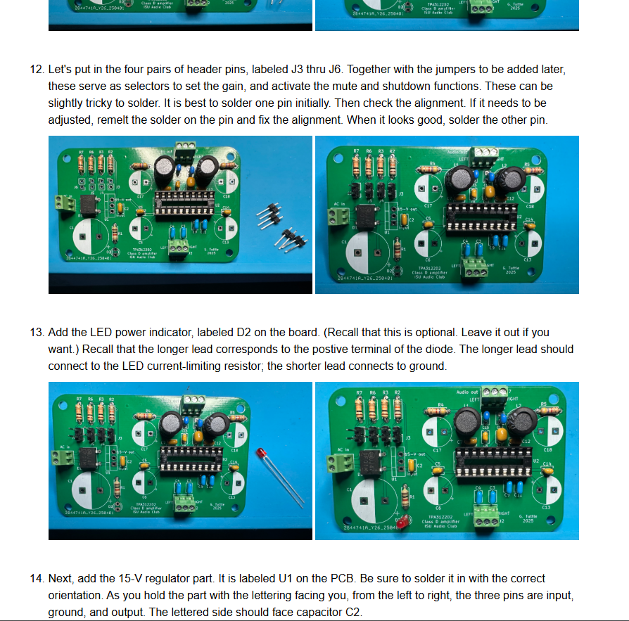
02 / Filters & controls
Output inductors and jumper headers add filtering and hardware configuration to the board.
03 / Completed board
The guide’s completed example brings the power section, filters, and amplifier IC together.
Circuit design and build guidance: Dr. Gary Tuttle / Audio Arduino Club. My role: building and learning from the club design.